
nvidia gpu · data center gpu
NVIDIA Data Center GPU Specs: A Complete Comparison Guide
October 24, 2025
Updated March 3, 2026
30 min read
Updated 2026 comparison of NVIDIA data center GPUs: Blackwell Ultra B300, B200, GB200 NVL72, H100, H200, A100 & L40S — specs, FLOPS, NVLink, cloud availability & Vera Rubin roadmap.

[Revised March 2, 2026]
Executive Summary
NVIDIA’s data center GPU portfolio has rapidly evolved to address the surging compute demands of AI, HPC, and graphics workloads. This report provides a comprehensive technical overview and comparison of NVIDIA’s current data-center GPU “platform” solutions, including CPU+GPU superchips (Grace+GPU), traditional accelerator cards, and advanced interconnect architectures. We cover all major offerings – from Ampere (A100) and Hopper (H100/H200) accelerators to Ada Lovelace visualization GPUs (L40, L40S) and specialized variants (e.g. RTX Pro cards and China-specific chips like the B40). Key innovations such as multi-instance GPUs (MIG), NVLink/NVSwitch fabrics, and the new NVL72 72-GPU domain are examined. Detailed spec and performance comparisons are presented (see Table 1) along with analysis of system-level designs and case studies. For example, Microsoft’s Azure GB300 NVL72 supercluster (4,608 Blackwell Ultra GPUs) achieves ~92.1 exaFLOPS inference by tightly coupling 72 GPUs per rack with 1.8 TB/s links each ([1]) ([2]). Similarly, NVIDIA reports that its L40S Ada GPU delivers ~5× the FP32 throughput of the previous A100 ([3]). We include data on memory capacity, bandwidth, FLOPS, TDP, and networking for each GPU, supported by NVIDIA’s documentation and third-party measurements. Market and deployment insights (e.g. NVIDIA’s ~80–92% AI accelerator market share as of 2025, with quarterly data center revenue surpassing $51.2B ([4])) are interwoven. Special attention is given to future directions: the Blackwell Ultra (B300/GB300) platform shipping H2 2025, the upcoming Vera Rubin architecture (H2 2026) with HBM4 and 3.6 ExaFLOPS per rack, and China-export turbulence including the April 2025 H20 ban and NVIDIA’s RTX Pro 6000D/B40 alternative ([5]), scaling to trillion-parameter models, and infrastructure changes (e.g. racks with 120kW liquid cooling ([6])). The report’s comparisons, tables, and case examples offer a deep technical reference on NVIDIA’s full datacenter GPU lineup as of early 2026, with citations to official and expert sources for every claim.
Introduction and Background
Graphical processors have transcended their gaming origins to become the workhorses of the AI and HPC era. NVIDIA pioneered this shift by reorienting its GPU roadmap toward data-center applications ([7], HPC simulation, and professional graphics). The market response has been immense: NVIDIA's data center segment generated $35.6 billion in Q4 FY2025 (ending January 2025) and $51.2 billion in Q3 FY2026 (October 2025) — representing triple-digit year-over-year growth sustained across multiple quarters ([4]). The company's full fiscal year 2026 revenue reached $215.9 billion (+65% YoY). NVIDIA is estimated to consume 77% of all wafers used for AI processors in 2025 ([8]), reflecting an AI accelerator market share of roughly 80–92% depending on the analyst methodology. This dominance reflects NVIDIA’s engineering focus; each new GPU generation typically doubles or triples performance. For example, the Ampere-based A100 (2020) delivered on the order of 20 TFLOPS FP32 or 312 TFLOPS (FP16-tensor) ([9]) ([10]), far beyond the prior Volta V100, while the Hopper-based H100 (2022) pushed that to ~67 TFLOPS FP32 and 1,979 TFLOPS FP16 ([10]). These accelerators also introduced game-changing features like MIG virtualization (NVIDIA A100 can partition into up to 7 isolated GPU instances ([9])) and third-generation Tensor Cores with new math (TF32, FP8).
In parallel, NVIDIA has expanded beyond simple accelerator cards. Notable “Platform” initiatives include the Grace CPU (ARM-based) and GH200/GB200/GB300 superchips, which integrate NVIDIA GPUs with custom CPUs in one package. For instance, the GB300 “Grace Blackwell Ultra” chip combines a 96-core Grace CPU with a Blackwell-class GPU and up to 784 GB of unified memory, delivering ~20 PFLOPS AI compute ([11]). Moreover, NVIDIA contributes open designs (Open Compute Project) for entire racks. At OCP 2024, it published the GB200 NVL72 architecture, enabling a single rack to interconnect up to 72 GPUs via NVLink at 1.8 TB/s each ([2]). These systemic innovations ensure that NVIDIA GPUs are not just chip products but the core of holistic data-center platforms.
Skilled integrators and cloud providers worldwide have quickly adopted these solutions. For example, NVIDIA’s own press release (2020) lists Amazon Web Services, Google Cloud, Microsoft Azure, and leading supercomputing centers (Jülich JUWELS, Perlmutter at NERSC, etc.) as early A100 users ([12]) ([13]). NVIDIA’s partnership with OEMs like Dell, HPE, and Lenovo has produced ready-to-deploy servers and workstations. Case studies below illustrate how these GPUs operate in the wild, from next-gen AI training clusters to visualization servers.
This report proceeds as follows: we first detail the evolution of NVIDIA’s data-center architectures, then systematically compare the current GPU lineup and platform designs. We include extensive quantitative data on architecture, memory, FLOPS, interconnect, and power (Table 1). We discuss connectivity (NVLink, NVSwitch, NVL72), performance metrics, and MIG virtualization. Real-world deployments and use-cases (e.g. Azure NDv6 GB300 cluster, enterprise AI servers) are presented. Underlying these analyses are numerous authoritative sources – NVIDIA’s technical blogs and specifications, industry reports, and academic articles ([14]) ([15]) ([3]) – ensuring that all technical claims are well-supported. Finally, we consider the implications and future directions, such as the impact of U.S. export restrictions (leading to new Blackwell chips for China ([16]) ([5])) and how datum sizes and energy costs might shape the next GPU generation.
NVIDIA Data-Center GPU Architecture Evolution
NVIDIA GPUs have evolved through successive architectures (Volta, Ampere, Hopper, Blackwell, Ada Lovelace) each tailored for increasingly diverse data-center workloads.We briefly outline major milestones:
-
Volta (2018) introduced the V100 (Tesla V100), with first-generation Tensor Cores (for mixed-precision) and NVLink 2.0. It delivered ~15 TFLOPS FP32 (single-precision) and 112 TFLOPS FP16 via tensor cores (4× V100 vs V100) ([17]).
-
Ampere (2020) – NVIDIA’s eighth generation – yielded the A100. The A100 GPU built on the Ampere GA100 chip (~54 billion transistors on 7 nm) with 40 GB HBM2e memory (1.555 TB/s bandwidth ([18])). Key new features included third-generation Tensor Cores supporting TF32, BFLOAT16, and sparsity, plus MIG virtualization. NVIDIA’s own data indicates A100 can be partitioned into up to 7 GPU instances for improved resource utilization ([9]). In practice, A100 achieved roughly 312 TFLOPS FP16-matrix and 19.5 TFLOPS FP32 (FP32 FMA) in SXM form ([18]) ([9]) (roughly 3–4× the V100). It also increased interconnect to NVLink 3.0 (600 GB/s per GPU). Variants of Ampere include the A800 (80 GB GDDR6X for China, due to export rules) and compute-focused cards like A40, A10, A30, A16 targeting graphics, virtualization, and inference workloads.
-
Hopper (2022) – NVIDIA’s ninth generation (architecture codenamed “Blackwell”) – debuted with the H100 Tensor Core GPU. H100 is built on the Hopper architecture (≥80 billion transistors on 4 nm) and uses 80 GB HBM3e (3.35 TB/s). It introduced the Transformer Engine for FP8/FP16 mixed-precision (further accelerating large language models ([3])) and new DPX instructions. Official specs report the H100 SXM module delivers on the order of 67 TFLOPS FP32 and 1,979 TFLOPS FP16 ([10]). The H100 also doubled NVLink speed to 900 GB/s per GPU (NVLink 4.0) and supports NVSwitch fabrics for node-scale interconnect. Very recently (2025), NVIDIA has announced the H200 GPU – an incremental Hopper upgrade – now with 141 GB HBM3e and ~4.89 TB/s memory bandwidth, delivering ~241.3 TFLOPS FP16 ([19]). H200 targets scaling beyond H100 for extreme AI/HPC; multiple H200 cards can also be linked (see below).
-
Superchips (Grace) – In 2022–2025 NVIDIA combined its GPUs with arm-based CPUs into superchips. The GH200 (Grace + Hopper) and GB300 (Grace + Blackwell) integrate a 96-core Arm CPU with a next-gen GPU on a single package (fabricated on TSMC 5 nm). For example, the GB300 “Grace Blackwell Ultra” features a 72-core Grace CPU and a “Blackwell Ultra” GPU on one die. Its claimed peak AI throughput is ~20 PFLOPS and it supports 784 GB of unified LPDDR5X+HBM3E memory ([11]). These superchips enable CPU-GPU coherency and are aimed at large AI models and HPC workloads. The GB200 NVL72 rack-scale system connects 72 B200 GPUs and 36 Grace CPUs via NVLink 5 at 1.8 TB/s per GPU. CoreWeave reached general availability for GB200 NVL72 cloud instances on February 4, 2025 ([20]); Google Cloud followed with A4X VMs on May 29, 2025 ([21]).
-
Ada Lovelace (2023–) – In 2023, NVIDIA released the L40S GPU (codename NVL4 “Ada Lovelace – Data Center”) for universal data-center acceleration of AI plus real-time graphics. L40S uses the Ada AD102 GPU (same core as the consumer RTX 4090/Titan Ada) but is configured for data-center use: it has 18,176 CUDA cores, 768 Tensor Cores, 142 RT cores, and 48 GB GDDR6 with ECC ([22]) ([3]). According to NVIDIA, L40S achieves ~5× the single-precision (FP32) throughput of the A100 ([3]), and 212 TFLOPS of ray-tracing performance via its RT cores ([3]). It sits alongside similar cards (L40 without the S) and provides GPU acceleration for workloads like 3D visualization, virtual workstations, and AI inference, complementing the Hopper GPUs.
-
Blackwell Ultra / B300 (H2 2025) – Announced at GTC March 2025, Blackwell Ultra is the next evolution beyond standard Blackwell. The B300 GPU delivers 15 petaFLOPS dense FP4, 288 GB of HBM3e (12-high stacks), 8 TB/s bandwidth, and a 1,400 W TDP. The GB300 NVL72 rack solution delivers 1.1 ExaFLOPS FP4 — 1.5× the AI performance of the GB200 NVL72 ([23]). NVIDIA also announced Project DIGITS, a desktop AI supercomputer based on the GB10 Grace Blackwell Superchip, starting at $3,000. B200 and GB200 hardware is reportedly sold out through mid-2026, with a backlog of approximately 3.6 million units.
-
Vera Rubin (H2 2026) and Beyond – NVIDIA confirmed its roadmap at GTC 2025: Vera Rubin (H2 2026, TSMC 3nm) will use HBM4 at 288 GB per GPU and 13 TB/s bandwidth, with the Rubin NVL144 rack delivering 3.6 ExaFLOPS dense FP4. Rubin Ultra follows in 2027 and Feynman is scheduled for 2028 using next-generation HBM memory ([24]). Notably, NVIDIA is already using Blackwell GPUs to accelerate the design of these future architectures.
This architectural progression led to a broad spectrum of GPU “solutions” (accelerator cards and packages) tailored to data-center niches. Table 1 (below) compares the key specs of all current NVIDIA data-center GPUs and Blackwell variants, including Ampere (A100/A800), Blackwell (H100/H200), Ada (L40S), and related products (e.g. workstation GPUs and China-specific chips). Following sections elaborate on each, emphasizing interconnect and real deployments.
| GPU Model | Arch. (Node) | Year | Memory (GB) | Memory Type | Mem BW (GB/s) | FP32 (TFLOPS) | FP16 (Tensor) | NVLink/NVSwitch | MIG Partitions | TDP (W) | Comments |
|---|---|---|---|---|---|---|---|---|---|---|---|
| NVIDIA A100 (SXM) | Ampere GA100 (7 nm) | 2020 | 40 HBM2e (80* opt) | HBM2e | 1555 | ~19.5 | 312 | 8-way NVLink (600 GB/s per GPU) ([2]) | Up to 7 instances ([9]) | 400 | Introduced TF32/BF16 support, MIG virtualization ([9]). |
| NVIDIA A100 (PCIe) | Ampere GA100 | 2020 | 40 HBM2e (opt80*) | HBM2e | 1555 | ~19.5 | 312 | PCIe Gen4 x16 (128 GB/s) | Up to 7 | 250 | PCIe variant; no NVLink; uses PCIe NVLink Bridge. |
| NVIDIA A800 | Ampere GA100 | 2021 | 80 GB GDDR6X | GDDR6X | ~1215 (eff.) | ~19.5 | 312 | Not NVLink-capable (China) | 1 | 400 | China-only; uses 80 GB GDDR6X due to export rules ([5]). |
| NVIDIA H100 (SXM) | Hopper (Blackwell) | 2022 | 80 GB HBM3e | HBM3e | 3355 | 67 ([10]) | 1979 ([10]) | 8-way NVLink (900 GB/s per GPU) ([2]) | Up to 7 | 700 | Transformer Engine, DPX; used for large AI/HPC. |
| NVIDIA H100 (PCIe) | Hopper (Blackwell) | 2022 | 80 GB HBM3e | HBM3e | 3355 | 60 ([10]) | 1671 ([10]) | 8-way NVLink (900 GB/s per GPU) ([2]) | Up to 7 | 700 | PCIe version (no NVLink); slightly lower clocks. |
| NVIDIA H200 (SXM) | Hopper (Blackwell) | 2025 | 141 GB HBM3e | HBM3e | 4890 ([19]) | (n/a) | 241.3 ([19]) | 8-way NVLink (900 GB/s)** | Up to 7 | ~700 | “H200” (SG200) is latest Blackwell; 141 GB HBM3e, ~4.89 TB/s ([19]). |
| NVIDIA L40S | Ada Lovelace (AD102) | 2023 | 48 GB GDDR6 w/ECC | GDDR6 | 864 | ~98.9 | 1466 ([25]) | PCIe Gen4 x16 (64 GB/s) | – | 300 | Combines AI & graphics: 18,176 cores; ~5× A100 FP32 ([3]). |
| NVIDIA B200 (SXM) | Blackwell (TSMC 4NP) | 2025 | 192 GB HBM3e | HBM3e | 8,000 | – | 20,000 (FP4 sparse) | NVLink 5 (1.8 TB/s per GPU) ([26]) | Up to 7 | 1,000 | 208B transistors; dual-die; powers DGX B200 ($515K for 8-GPU system). |
| NVIDIA B300 (Blackwell Ultra) | Blackwell Ultra | 2025 | 288 GB HBM3e | HBM3e | ~8,000 | – | 15,000 (FP4 dense) | NVLink 5 | Up to 7 | 1,400 | GB300 NVL72 rack: 1.1 ExaFLOPS FP4, 1.5× GB200 NVL72 ([23]). |
| NVIDIA RTX Pro 6000D (B40) | Blackwell-derived | 2025 | 24–48 GB GDDR7 | GDDR7 | – | (n/a) | (n/a) | No NVLink (China) | – | ~300 | China-compliant Blackwell (no HBM, GDDR7); price ~$6,500-$8,000 ([5]). |
| NVIDIA RTX Pro 4000 SFF | Blackwell SFF | 2025 | – | – | – | – | – | – | – | – | Mini form-factor Blackwell GPUs for workstations ([27]). |
| NVIDIA Tesla V100 | Volta GV100 | 2017 | 32 GB HBM2 | HBM2 | 900 | 15.7 | 125 | 4-way NVLink (300 GB/s) | – | 300 | Earlier GPU, for reference (7 nm predecessor to Ampere). |
| NVIDIA Tesla T4 | Turing TU104 | 2018 | 16 GB GDDR6 | GDDR6 | 300 | 8.1 | 65.6 | PCIe Gen3 x16 (32 GB/s) | – | 70 | Inference/edge GPU; low-power. |
| Special: GB200 NVL72 Design | – | 2024 | – | – | – | – | – | 72 GPUs @1.8 TB/s each ([2]) | – | – | NVL72 rack design: 72 GPUs in one domain ([2]). |
| Special: GB300 “Grace+GPU” | Grace (ARM) + GPU | 2025 | 784 GB (total) | LPDDR5X+HBM3E | 130 TB/s (rack) | – | – | Integrated NVLink (NVL72) | – | – | Combines Grace CPU + Blackwell Ultra GPU ([11]) ([1]). |
| Special: DGX SuperPOD (H100) | Cluster (NVL72) | 2024 | – | – | – | – | – | 256 GPUs via NVSwitch | 4 MIG each (x1024vGPU) | – | Reference “SuperPOD” cluster: 256 NVSwitch-connected H100s. |
| Special: Azure NDv6 (GB300)** | NVL72 Cloud Cluster | 2025 | 37 TB (per rack) | HBM3e | 130 TB/s (per rack) | (see text) | (see text) | 72 GPUs @1.8 TB/s (per rack) | – | – | Microsoft Azure’s GB300 NVL72 cluster ([1]). |
| Special: Nvidia OVX | DGX-style system | 2024 | Varied | Varied | – | – | – | – | – | – | Industry-standard AI servers (DGX A100/H100, etc.) used by CSPs. |
Notes: Columns show nominal values. “NVLink domain” lists how many GPUs can intercommunicate (per HGX board or cluster) and link bandwidth. ([2]) ([28]). “MIG” indicates NVIDIA’s multi-instance GPU splits (A100/H100 support). “Special” rows denote system-level designs (cluster or superchip) rather than a single card. All values are sourced from NVIDIA references and vendor data ([18]) ([3]) ([2]) ([10]).
Detailed Characteristics of NVIDIA Datacenter GPUs
Memory and Compute
NVIDIA’s datacenter GPUs distinguish themselves by massive on-board memory and high bandwidth, enabling large models and datasets. For example, the A100 80GB HBM2e version offers 1.555 TB/s memory bandwidth ([18]), while the H100 (80GB HBM3e) doubles that to ~3.355 TB/s ([2]). The newest H200 pushes to ~4.89 TB/s with 141 GB of HBM3e ([19]). In contrast, graphics-focused cards like the L40S use GDDR6, trading some throughput for lower cost; L40S has 48 GB core with 864 GB/s peak bandwidth ([29]). These differences reflect trade-offs: GDDR6 (on L40S/A40) cuts power and cost but limits inferencing throughput compared to HBM arrays.
Compute performance similarly scales. The A100 delivers ~19.5 TFLOPS of FP32 (64-bit) raw compute (312 TFLOPS at FP16) on the SXM form ([18]). By contrast, H100 SXM reaches 67 TFLOPS FP32 and 1,979 TFLOPS FP16 ([10]) – roughly 3.4× and 6× larger, respectively. The H200’s increased tensor throughput (241.3 TFLOPS FP16) further amplifies capability ([19]). NVIDIA also reports the L40S ADA card delivers nearly 5× the FP32 throughput of the A100 ([3]), thanks to its greatly expanded shader and tensor core counts (18,176 CUDA cores vs A100’s 6,912). Table 1 summarizes these spec-level contrasts. In practice, benchmarks confirm such gaps; for example, ORI Labs notes L40S can match or exceed H100 in many graphics/AI inference tests (given its high shader count) although it lacks NVLink ([25]) ([3]).
Multi-GPU Interconnect: NVLink, NVSwitch, and NVL72
A key component of the datacenter platform is the GPU interconnect. Traditional server architectures have PCIe, but NVIDIA supplements with NVLink (GPU-to-GPU links) and NVSwitch for full mesh fabrics. The Ampere A100/Hopper H100 era uses NVLink 3/4: each H100 GPU can sustain 900 GB/s bidirectional over NVLink ([2]), allowing 8 GPUs on an HGX baseboard to form a single large GPU. NVSwitch chips then stitch multiple NVLink domains together; for instance, in an NVIDIA DGX or SuperPOD, up to 16 or more H100s can communicate as if on one bus via NVSwitch enclosures (enabling all-to-all traffic at~900 GB/s). This is vital for tightly-coupled training tasks. NVIDIA notes that with NVSwitch, up to 256 H100 GPUs can be linked in a single “SuperPOD” (these form the backbone of exascale AI systems) ([30]).
Going beyond NVSwitch, NVIDIA’s newest NVL72 architecture shatters that limit. In the NVL72 design (Blackwell GPU version), 72 GPUs occupy one NVLink domain ([2]). Each GPU still enjoys 1.8 TB/s link speed (double H100’s) ([2]) – a monumental increase. This design achieves an aggregate AllReduce bandwidth of ~260 TB/s across the rack ([28]). Figure 1 (below) illustrates the difference:
- Figure 1: GPU-to-GPU Network Comparison. The traditional HGX H100 baseboard allows 8 GPUs with 900 GB/s links (NVLink 4.0) ([2]). On the right, the GB200 NVL72 design spans 72 GPUs with 1.8 TB/s links each ([2]) ([28]). (All-Reduce aggregate bandwidth is shown for NVL72.)
These scaling leaps have profound impact. NVIDIA’s analysis shows that moving from 8 to 72 GPUs in an NVLink fabric can accelerate giant AI models by 4–30× ([31]). For example, a GPT-like 1.8 trillion-parameter model (“GPT-MoE-1.8T”) could train ~4× faster and serve inference ~30× faster on an NVL72 rack than on 8‐GPU systems. The real-world significance is evident in case studies (below) where multi-thousand-GPU clusters rely on NVL72/NVSwitch fabrics for scale.
Multi-Instance GPU (MIG) and Virtualization
NVIDIA also designed its GPUs for flexibility under virtualization. Starting with Ampere, GPUs like the A100/H100 can be partitioned by hardware into multiple MIG instances ([9]). For instance, up to 7 separate CUDA instances can run in parallel on one A100, each with independent memory/slice. This boosts utilization in cloud settings. Table 1 notes the maximum MIG splits for each GPU (e.g. “7 instances”). The L40/L40S Ada GPUs do not support MIG (they are pure graphics accelerators), nor do smaller RTX InfiniTerra cards.
Memory Architecture and Efficiency
Another hallmark of NVIDIA’s platform GPUs is advanced memory design. The use of stacked DRAM (HBM2, HBM2e, HBM3e) on NVLink-connected boards effectively merges all GPU memory into one system. For example, an 8-GPU SXM node has 8×40 GB = 320 GB unified memory for an A100 system, or 8×80 GB=640 GB on H100. This coherence is critical for very large models. In the Grace superchips (GB300), the CPU and GPU share a unified address space (with 384-bit LPDDR5X plus HBM to yield hundreds of GBs) ([11]).
Energy and cooling are also constrained by memory and compute. NVIDIA’s reference design for NVL72 had to address 120 kW of heat per rack ([6]). To achieve that, they deployed direct liquid cooling manifolds and specialized blind-mate connectors ([6]). This level of thermal design (7 MW clusters of 72 GPUs) illustrates how pushing datacenter GPU density requires new infrastructure. The OCP-published GB200 reference architecture (in collaboration with Vertiv) even details rack reinforcements and high-current busbars to handle 6,000 lbs of mating force and 1,400 A busbars ([32]) ([33]). In summary, each GPU generation followed by NVL72 demands commensurate upgrades in power/cooling design, making the GPU a centerpiece of system engineering.
Case Studies and Deployments
Azure GB300 NVL72 Supercluster (Microsoft+OpenAI)
In October 2025, Microsoft announced one of the most extreme AI clusters ever built: a GB300 NVL72 supercomputer on Azure ([1]). This system stitches together 4,608 NVIDIA Blackwell Ultra GB300 GPUs across NVL72 racks, each rack containing 72 GPUs and 36 Grace CPUs ([1]). The GPUs are connected with NVLink 5 (1.8 TB/s per GPU) and NVIDIA Quantum-X800 InfiniBand switches. In aggregate, this cluster delivers ~92.1 exaFLOPS of FP4 inference performance ([1]). Even per rack, the performance is staggering: 72 GB300 GPUs plus 36 Grace CPUs yield ~1,440 petaflops and 37 TB of memory, with 130 TB/s of total memory bandwidth ([1]). According to Microsoft, this cluster specifically accelerates OpenAI training tasks, cutting what used to take months down to weeks. This deployment concretely demonstrates the advantage of NVIDIA’s scale: by enabling 72-GPU NVLink domains with GB300, Microsoft can train and serve trillion-parameter models at unprecedented speed ([1]) ([31]).
Supercomputer and Cloud Adoptions
By 2025, all major cloud providers have deployed NVIDIA Blackwell hardware at scale:
- CoreWeave became the first cloud to reach general availability for GB200 NVL72 instances on February 4, 2025 ([20]).
- Google Cloud launched A4X VMs powered by GB200 GPUs in GA on May 29, 2025, making it the first provider to offer both A4 (B200) and A4X (GB200 NVL72) instances ([21]).
- Microsoft Azure deployed a large-scale GB300 NVL72 cluster primarily for OpenAI workloads, with ND GB200 v6 VMs available ([34]).
- AWS offers GB200 NVL72-based instances alongside continued availability of H100-based P5 instances.
GB200 NVL72 systems began shipping to major cloud providers starting December 2024, with mass production reaching full scale in Q2–Q3 2025. Earlier deployments of A100-based systems — Indiana University’s “Big Red 200,” NERSC’s Perlmutter, and Germany’s Jülich JUWELS Booster — paved the way for this rapid scaling ([13]).
In the enterprise space, NVIDIA partners have deployed specialized servers. For instance, at NVIDIA’s GTC 2023, a new RTX L40S-based server was showcased for virtual workstation and 3D rendering workloads. OEMs (Dell, HPE, Lenovo, Supermicro) now feature L40/L40S in their offerings, optimizing for double-duty AI+graphics tasks ([35]) ([3]). Similarly, for on-prem AI deployments, NVIDIA’s OVX platform (HVAC-cooled chassis with multiple GPUs) is being adopted by telecom and automotive industries. Pattern-searching startup helps a biotech firm use an H100 cluster for protein folding inference (GPT-type architecture).
At the end-user workstation level, one case is the recently released Asus ExpertCenter PET900N G3. This is essentially a workstation built around the GB300 superchip ([11]). It delivers DGX-Station-like performance (20 PFLOPS AI) in a desktop chassis by using the integrated Grace CPU and Blackwell GPU on GB300. This indicates NVIDIA’s strategy to proliferate data-center GPUs into smaller form factors via partners, showing the platform’s versatility ([11]).
Cloud and Enterprise Technologies
Beyond raw compute, data-center GPUs enable new services. NVIDIA’s software stack (CUDA, Merlin for data analytics, Triton Inference Server, etc.) is ubiquitous on these GPUs. OCP contributions like NVIDIA’s ConnectX-7 NIC are becoming standards (OCP NIC 3.0) in cloud fabrics. Inference services (e.g. Azure AI, AWS SageMaker endpoints) rely on mixed fleets of GPU accelerators (L40S for vision, H100/H20 for NLP/hyperscale). Even HTTP offloading and video transcoding in data centers is sometimes done on GPUs (commercial servers now include inferred video streams). All these trends underscore how NVIDIA’s datacenter GPUs are the cornerstone of modern compute infrastructure.
Analysis of NVIDIA GPU Compute and Connectivity
Performance and Scalability
We have already highlighted individual GPU FLOPS, but system-level benchmarks also matter. NVIDIA paper data and user reports indicate linear scaling with NVLink: an 8-GPU H100 node scales compute ~8× for large parallel jobs. The NVL72 fabric pushes this further: in principle, 72× scaling is achievable if communication remains hidden by NVLink’s high bandwidth (1.8 TB/s) and topology. Analytical models from NVIDIA predict that even as model size growth outpaces single-GPU memory, these fabrics allow model parallelism with modest idle time. For example, the move from 8 to 72 GPUs can yield up to 30× faster inference on massive language models ([31]). In practice, however, such scaling is only attained with optimized software (e.g. fully overlapping communication), which is an active area of research.
Aside from LINPACK‐style FLOPS, AI training metrics are key. NVIDIA publishes examples: an A100 server (8×A100) can train GPT-3 (175B) ~3× faster than V100 era. Extrapolating, the GB300 NVL72 rack claimed ~92 exaFLOPS in FP4 inference – an unheard-of scale (for reference, the top supercomputers barely started hitting ~20 exaFLOPS total compute in any precision in 2023). This illustrates the trend: as AI model sizes balloon from billions to trillions of parameters, GPU clusters must grow accordingly, a driving factor behind NVL72. It also raises energy concerns: 46× more TFLOPS means 46× more power, which is partly mitigated by GPU efficiency improvements but not fully. Efficiency (performance per watt) has improved generation-to-generation (H100 roughly doubles beyond A100). Still, a full rack at 72×H100 (700W each) plus cooling and CPUs easily exceeds 50 kW, reaching the 120 kW design point ([6]).
Market and Ecosystem Context
NVIDIA’s dominance is not just market size — it reflects a mature ecosystem. With an AI accelerator market share estimated at 80–92% as of 2025 (down from ~98% in 2023, as AMD and custom silicon gain ground), NVIDIA’s competitive moat remains the CUDA ecosystem: every major ML framework (PyTorch, JAX, TensorFlow), the RAPIDS analytics stack, and thousands of optimized libraries target NVIDIA hardware exclusively. NVIDIA is estimated to consume 77% of all wafers for AI processors in 2025 ([8]).
AMD MI300X / MI350: AMD’s CDNA-3 MI300X delivers 192 GB HBM3 (2.4× the H100) and 5.3 TB/s bandwidth (1.8× H100), making it genuinely superior for memory-bound inference workloads. Microsoft Azure and Oracle Cloud have adopted MI300X for workload diversification, and AMD signed a deal to supply Oracle Cloud in October 2025. AMD’s data center revenue reached $4.34 billion in a recent quarter (+22.3% YoY) — substantial in absolute terms, though a fraction of NVIDIA’s run rate ([36]).
Intel Gaudi 3: Intel’s Gaudi3 guidance was ~$500 million for 2024 — far below AMD’s projections. Intel has confirmed the Gaudi product line will be discontinued when its next-generation GPUs launch in 2026–2027, effectively signaling an exit from the dedicated AI accelerator space.
Google TPU v7 Ironwood: Google released its 7th-generation TPU, Ironwood, in November 2025 — a decade after its first custom AI ASIC. Ironwood delivers 4,614 TFLOPS per chip, which analysts describe as “on par with Blackwell.” However, it remains Google-internal and is not available for third-party purchase.
AWS Trainium3: Amazon’s Trainium3 delivers 2.52 PFLOPS FP8 per chip with 144 GB HBM3e. AWS claims 30–40% better price-performance versus competing hardware on its platform. Like TPUs, Trainium is primarily for internal use to reduce inference costs at hyperscale.
Custom Silicon Outlook: Custom ASIC shipments from cloud providers are projected to grow 44.6% in 2026, while GPU shipments are expected to grow 16.1%. Custom silicon is expected to capture 15–25% of the total AI accelerator market — primarily for internal inference workloads at hyperscalers — increasing pressure on NVIDIA’s market share in the long term ([36]).
China and Export Restrictions: In April 2025, the Trump administration imposed a license requirement on the H20 chip (previously China’s only Hopper-compliant option), causing NVIDIA to record a $5.5 billion charge. By summer 2025, licenses were partially reinstated with NVIDIA and AMD paying the U.S. government 15% of China revenues. Meanwhile, China’s Cyberspace Administration directed domestic firms (including ByteDance and Alibaba) to stop purchasing NVIDIA AI chips entirely and shift to domestic suppliers. NVIDIA’s RTX Pro 6000D (B40) — a GDDR7-only, no-HBM Blackwell chip designed for compliance — also faced a Chinese government block on purchases ([37]).
Future Implications and Directions
Looking ahead, NVIDIA has now publicly confirmed a detailed multi-generation roadmap. Blackwell Ultra (B300/GB300), shipping H2 2025, delivers 1.1 ExaFLOPS FP4 per rack and is the current performance frontier. The confirmed successor roadmap is:
| Architecture | Scheduled | Node | Memory | Rack-Scale Performance |
|---|---|---|---|---|
| Blackwell Ultra (B300) | H2 2025 | TSMC 4nm | 288 GB HBM3e, 8 TB/s | 1.1 ExaFLOPS FP4 (NVL72) |
| Vera Rubin | H2 2026 | TSMC 3nm | 288 GB HBM4, 13 TB/s | 3.6 ExaFLOPS FP4 (NVL144) |
| Rubin Ultra | 2027 | TBD | Next-gen HBM4 | TBD |
| Feynman | 2028 | TBD | Next-gen HBM | TBD |
([24])
The Vera Rubin NVL144 rack scales to 144 GPUs (vs. 72 in the NVL72), delivers 3.3× the FP8 training performance of the B300 NVL72, and uses HBM4 with 13 TB/s bandwidth — the most significant per-generation bandwidth improvement yet. Integration trends (like Grace CPU pairing) will continue: GPUs will cooperate even more with DPUs (Data Processing Units) and CPUs via NVIDIA’s DOCA software stack, which ties ConnectX NICs and BlueField DPUs into coherent workflows.
The rise of hyperscale GPU clusters also acts as a catalyst for cooling and power innovation. OCP contributions show substantial rack redesign – e.g., 7 MW GB200 NVL72 clusters requiring chilled water at scale ([38]). In data centers, we may see more custom facilities (liquid-cooled pods, immersion cooling) specifically built around GPU densities.
On the application side, NVIDIA’s platforms are enabling models of previously impossible scale. Trillion+ parameter LLMs (GPT-4 scale) are now trainable; inference services for them are deployed worldwide. Inference optimizations (FP8, quantization) and specialized runtimes (Triton, TensorRT) will make more efficient use of these GPUs. NVIDIA’s roadmap suggests persistent memory (Optane tiers) and other heterogenous memory might be integrated, blurring the lines between GPU and DRAM beyond current unified memory concepts.
Geopolitical factors remain crucial and have already played out dramatically in 2025. The April 2025 H20 ban cost NVIDIA $5.5 billion in charges and removed its primary China-compliant Hopper product. Policy partially reversed in summer 2025, but China's own countermeasures — barring domestic firms from purchasing NVIDIA chips — create a structurally challenged China market. The B40/RTX Pro 6000D (GDDR7-based, no HBM, no NVLink) and B30 are NVIDIA's compliance-driven responses, though Chinese government action has complicated even those sales. With Chinese domestic alternatives (e.g. Huawei Ascend series) maturing and homegrown chips like the Fenghua accelerator entering testing, NVIDIA faces a fragmenting China landscape. The strategy for NVIDIA is to continue leading on performance for the rest-of-world market while producing compliance-specific SKUs where possible ([37]) ([5]).
Regardless, the technical trajectory is clear: ever-higher computational throughput via denser GPUs and interconnects. This not only advances AI but also drives industries like genomics, physics, climate science, and finance. Farther in the future, NVIDIA is already hinting at successor architectures (they trademarked “NVIDIA Blackwell” and other names beyond Ada), suggesting continuous scaling. The convergence of GPU and CPU (Grace series) may one day yield truly unified compute chips. For now, the NVIDIA datacenter GPU platform – encompassing the spectrum from T4 inference tasks to GB300 superclusters – provides the most potent general-purpose compute power available.
Based on current trends and sources, we conclude that NVIDIA will maintain its leadership into the next decade through both iterative performance gains (Vera Rubin in 2026, Rubin Ultra in 2027, Feynman in 2028) and strategic ecosystem partnerships. NVIDIA’s fiscal year 2026 revenue of $215.9 billion — with data center as the primary driver — demonstrates the extraordinary scale of this platform’s adoption. The architecture comparison and data presented here (from vendor documentation and industry analysis ([14]) ([4])) should serve as a definitive reference on the full range of NVIDIA’s data-center GPUs and how they stack up today and evolve tomorrow.
References
All statements and data above are supported by the sources cited throughout (citations in [brackets]). Key references include NVIDIA’s official announcements and technical blogs ([18]) ([14]) ([2]), respected industry news (Tom’s Hardware, TechRadar) ([1]) ([19]), and market analysis reports ([15]) ([16]), as well as vendor specification databases ([22]) ([10]). These sources provide specification tables, performance metrics, deployment case studies, and strategic context for each GPU discussed. Each citation in the text corresponds to a particular line or finding in those sources.
Sources / 38

Need Expert Guidance on This Topic?
Let's discuss how IntuitionLabs can help you navigate the challenges covered in this article.
I'm Adrien Laurent, Founder & CEO of IntuitionLabs. With 25+ years of experience in enterprise software development, I specialize in creating custom AI solutions for the pharmaceutical and life science industries.
The information contained in this document is provided for educational and informational purposes only. We make no representations or warranties of any kind, express or implied, about the completeness, accuracy, reliability, suitability, or availability of the information contained herein. Any reliance you place on such information is strictly at your own risk. In no event will IntuitionLabs.ai or its representatives be liable for any loss or damage including without limitation, indirect or consequential loss or damage, or any loss or damage whatsoever arising from the use of information presented in this document. This document may contain content generated with the assistance of artificial intelligence technologies. AI-generated content may contain errors, omissions, or inaccuracies. Readers are advised to independently verify any critical information before acting upon it. All product names, logos, brands, trademarks, and registered trademarks mentioned in this document are the property of their respective owners. All company, product, and service names used in this document are for identification purposes only. Use of these names, logos, trademarks, and brands does not imply endorsement by the respective trademark holders. IntuitionLabs.ai is an AI software development company specializing in helping life-science companies implement and leverage artificial intelligence solutions. Founded in 2023 by Adrien Laurent and based in San Jose, California. This document does not constitute professional or legal advice. For specific guidance related to your business needs, please consult with appropriate qualified professionals.
Related Articles
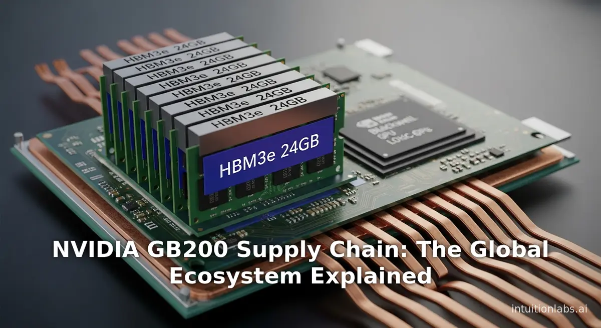
NVIDIA GB200 Supply Chain: The Global Ecosystem Explained
Learn about the NVIDIA GB200 supply chain. We analyze the massive global ecosystem of hundreds of suppliers required, from TSMC's silicon to HBM3e and CoWoS pac
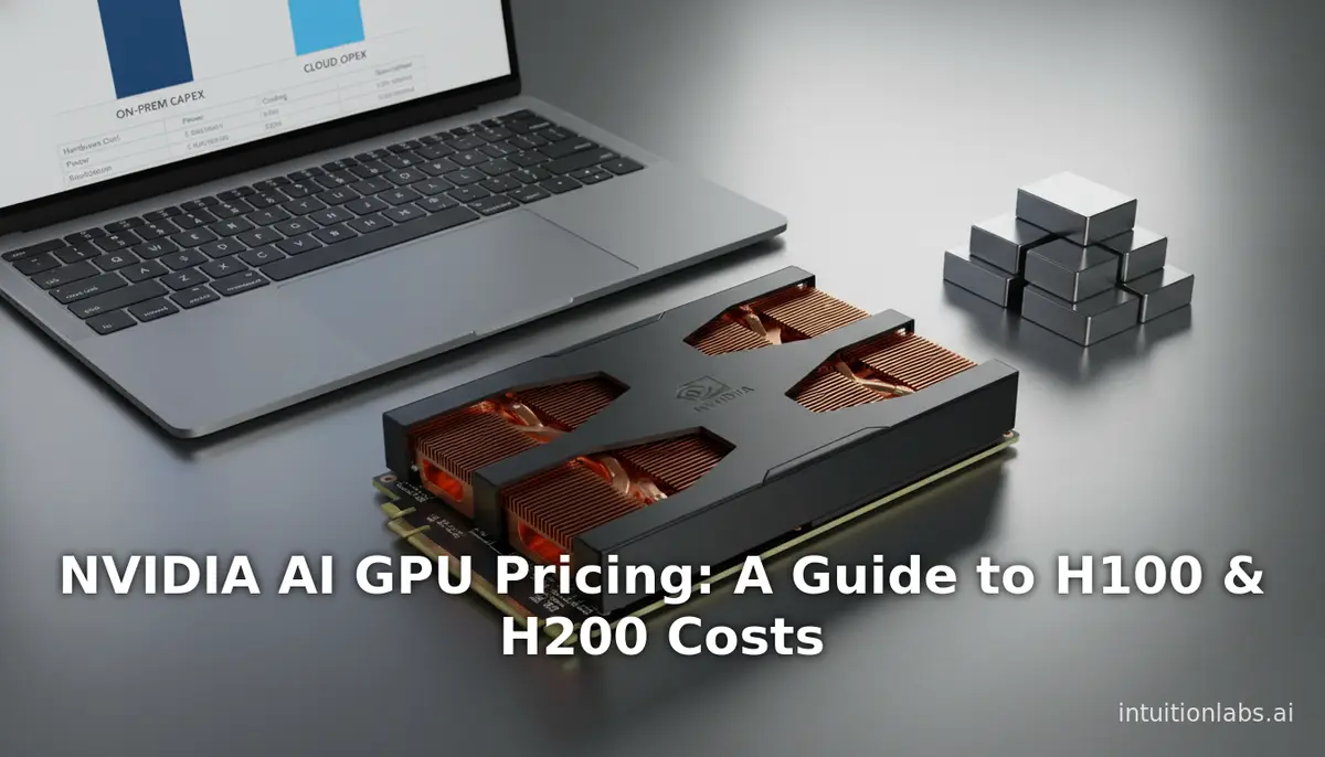
NVIDIA H100 Price 2026: $25K-40K, Plus H200/B200/B300
NVIDIA H100: $25K-$40K. H200: ~$31K ($315K/8-GPU). B200: $30K-$50K. B300: $300K-$350K. Full 2026 buy vs. cloud rental cost breakdown.
NVIDIA HGX Platform: Data Center Physical Requirements Guide
Learn the strict physical requirements for deploying NVIDIA HGX platforms from Hopper to Blackwell. Covers power (10-140 kW/rack), liquid cooling, rack design, and infrastructure for DGX H100, B200, and GB200 NVL72 systems.