
nvidia nvlink · gpu interconnect
NVIDIA NVLink Explained: A Guide to the GPU Interconnect
October 22, 2025
35 min read
Learn about NVIDIA NVLink, the high-speed GPU interconnect from NVLink 1.0 through NVLink 6.0 (Rubin). This guide covers architecture, bandwidth specs, NVSwitch, NVLink Fusion, and comparisons with AMD Infinity Fabric, CXL, and UALink.
[Revised February 28, 2026]
Executive Summary
NVIDIA NVLink is a revolutionary high-speed GPU interconnect architecture that fundamentally transforms the way graphics accelerators are coupled with CPUs and with each other. Introduced in 2016 with the NVIDIA Pascal™ P100 GPU, NVLink provides up to 5× the bandwidth of PCIe 3.0 x16 per link ([1]) ([2]). By scaling to multiple NVLink lanes per GPU, NVLink delivers order-of-magnitude higher data rates than traditional PCIe (e.g. an NVIDIA Tesla P100 achieves 160 GB/s bidirectional vs ~32 GB/s over PCIe Gen3×16 ([1])). As a result, systems built on NVLink (often paired with NVIDIA’s NVSwitch fabric) can achieve hundreds of GB/s to TB/s GPU-to-GPU bandwidth, unleashing vastly higher application performance in multi-GPU and CPU–GPU workloads. NVLink enables coherent shared memory across processors (already deployed in DOE pre-exascale supercomputers Summit and Sierra ([2])), effectively treating GPU memory and CPU memory as part of a unified address space. This dramatically speeds up workloads with frequent GPU-GPU and GPU-CPU communication (e.g. distributed AI training, large-scale simulations, and unified-memory applications).
In short, NVLink is revolutionary because it breaks the former PCIe bottleneck for GPU interconnects. It offers orders of magnitude greater bandwidth and new memory-coherency capabilities that were not possible with standard PCIe or earlier interconnects. For example, Oak Ridge’s Summit supercomputer (2018) uses NVLink to connect IBM POWER9 CPUs with 27,648 NVIDIA Volta V100 GPUs, yielding 8× the performance of its predecessor Titan on only a quarter of the nodes ([3]) ([2]). More recently, in 2025 Microsoft deployed a 4,608-GPU NVLink-connected cluster on Azure (72 GPUs per rack with IBM Grace CPUs) achieving 92.1 exaFLOPS of FP4 inference by tying GPUs with NVLink 5 fabric ([4]). These breakthroughs – along with NVLink’s ability to scale (via NVIDIA NVSwitch for intra-node all-to-all connectivity and NVLink-based networks for inter-node links) – enable new classes of applications and system designs. Overall, NVLink and its ecosystem (NVSwitch, NVLink networking, NVLink Fusion, etc.) represent a paradigm shift from commodity CPU buses to GPU-centric SMP-like architectures, unlocking massive performance and scalability gains in modern AI and HPC systems ([5]) ([6]).
Introduction and Background
The emergence of GPU-accelerated computing has been a key driver of the AI and HPC revolution. Modern supercomputers and data centers use thousands of NVIDIA GPUs to train deep neural networks, simulate scientific models, and process large data sets. However, the PCI Express (PCIe) bus – the standard interconnect for attaching accelerators to CPUs in x86 servers – has become a critical bottleneck. PCIe Gen3/4, with about 16–32 GB/s of bidirectional throughput per x16 link, cannot keep up with the massive data rates that GPUs can sustain internally. As GPU computational power and on-chip memory bandwidth have skyrocketed, feeding data between GPUs and CPUs (and between GPUs) over PCIe became a severe constraint in multi-GPU systems ([1]) ([7]).
To overcome this limitation, NVIDIA developed NVLink, a proprietary point-to-point interconnect for GPUs and CPUs. NVLink was first announced in 2014 and publicly introduced with the Pascal-generation Tesla P100 accelerator in 2016. It was designed explicitly to increase GPU communication bandwidth and enable unified memory architectures. In contrast to PCIe’s shared bus, NVLink provides a scalable mesh of high-bandwidth links, with each link capable of tens of gigabytes per second in each direction. Multiple NVLink links can be combined (”bonded”) to yield very high aggregate bandwidth between devices. Crucially, NVLink also adds hardware support for cache coherence and unified virtual addressing (across CPU and GPU) in later generations, enabling GPUs and Power CPUs to access each other’s memories as peers ([2]) ([8]). This blurs the boundary between CPU and GPU memory, letting large “model” or “domain” data sets span both memory systems without constant housekeeping by software.
In effect, NVLink brings GPU connectivity into the realm of symmetric multiprocessing (SMP). As noted by The Next Platform (2016), NVLink “lashing GPUs to CPUs” is “something as transformative as SMP was for CPUs” ([5]). For the first time, GPUs in a node can be wired together with bandwidth and latency on par with accessing CPU memory. The result has been revolutionary: multi-GPU computing that previously had to treat GPUs as isolated accelerators now becomes a tightly-coupled supercomputer on each node. NVLink’s evolution has been matched to each NVIDIA GPU generation, with each new NVLink generation pushing performance far above PCIe (see Table 1).
| NVLink Gen | GPU Architecture (Year) | Link Speed | Links per GPU | Total Bandwidth (GB/s, bidirectional) | Notes/Features |
|---|---|---|---|---|---|
| NVLink 1.0 | Pascal P100 (2016) | 20 GB/s (per link per direction) (40 GB/s bidirectional) | 4 | 160 GB/s ([9]) ([2]) | First NVLink; enables GPU–GPU and GPU–CPU (Power8) links; used in early NVLink-CPU systems (IBM POWER8+) |
| NVLink 2.0 | Volta V100 (2017) | 25 GHz (GT/s), 25 GB/s per direction (50 GB/s bidirectional) ([8]) | 6 | 300 GB/s ([8]) | Added cache coherence and unified address; supported by IBM POWER9; Tesla V100: 6 links |
| NVLink 3.0 | Ampere A100 (2020) | 50 GB/s per direction per link | 6 | 600 GB/s† | A100: Ampere’s GPU (third-gen NVLink); \~2× bandwidth of V100; used in DGX A100, NVIDIA HGX |
| NVLink 4.0 | Hopper H100 (2022) | 50 GHz (100 GB/s per direction per link) ([10]) | 12 | 900 GB/s ([11]) ([10]) | H100: 4th-gen NVLink; triple PCIe Gen5 speed ([10]); enables NVLink Switch System; NVLink network |
| NVLink 5.0 | Blackwell B200/GB200 (2024–25) | 100 GB/s per link per direction | 18 | 1,800 GB/s ([12]) | GB200 NVL72: 72 GPUs + 36 Grace CPUs per rack; 130 TB/s system bandwidth; supports up to 576 GPUs in non-blocking fabric |
| NVLink 6.0 | Rubin (2026) | 3,600 GB/s per GPU (2× NVLink 5) | TBD | 3,600 GB/s ([13]) | Vera Rubin NVL72: 72 Rubin GPUs + 36 Vera CPUs; 260 TB/s rack bandwidth; up to 10× inference cost reduction vs Blackwell; expected H2 2026 |
Table 1: Comparison of NVIDIA NVLink generations. Link speeds and aggregate bandwidths are per GPU; NVLink doubles as the GPU–GPU and GPU–CPU interconnect. NVLink 1–4 correspond to Pascal, Volta, Ampere, and Hopper GPU architectures; NVLink 5 to Blackwell; and NVLink 6 to the upcoming Rubin platform ([9]) ([11]) ([13]).
NVLink’s raw bandwidth improvement over PCIe is dramatic. For example, NVIDIA’s own press materials highlight that the Pascal P100 GPU’s NVLink interconnect delivers about 160 GB/s bidirectional – roughly 5× the throughput of a PCIe 3.0 x16 slot (∼31.5 GB/s) ([1]). Similarly, the NVLink in a Hopper H100 line card can provide ~100 GB/s per link (50 GB/s each way), so that with multiple NVLinks the total per-GPU interconnect bandwidth reaches 900 GB/s ([11]) ([10]) – compared to only 128 GB/s for a single PCIe Gen5 x16 link (32 GB/s each way). In short, NVLink line-speeds are measured in tens of gigabytes per second per lane, far eclipsing the externally-facing CPU bus. This lets GPUs exchange data almost as quickly as they pull from their own onboard HBM2/3 memory, unlocking new data-driven algorithms.
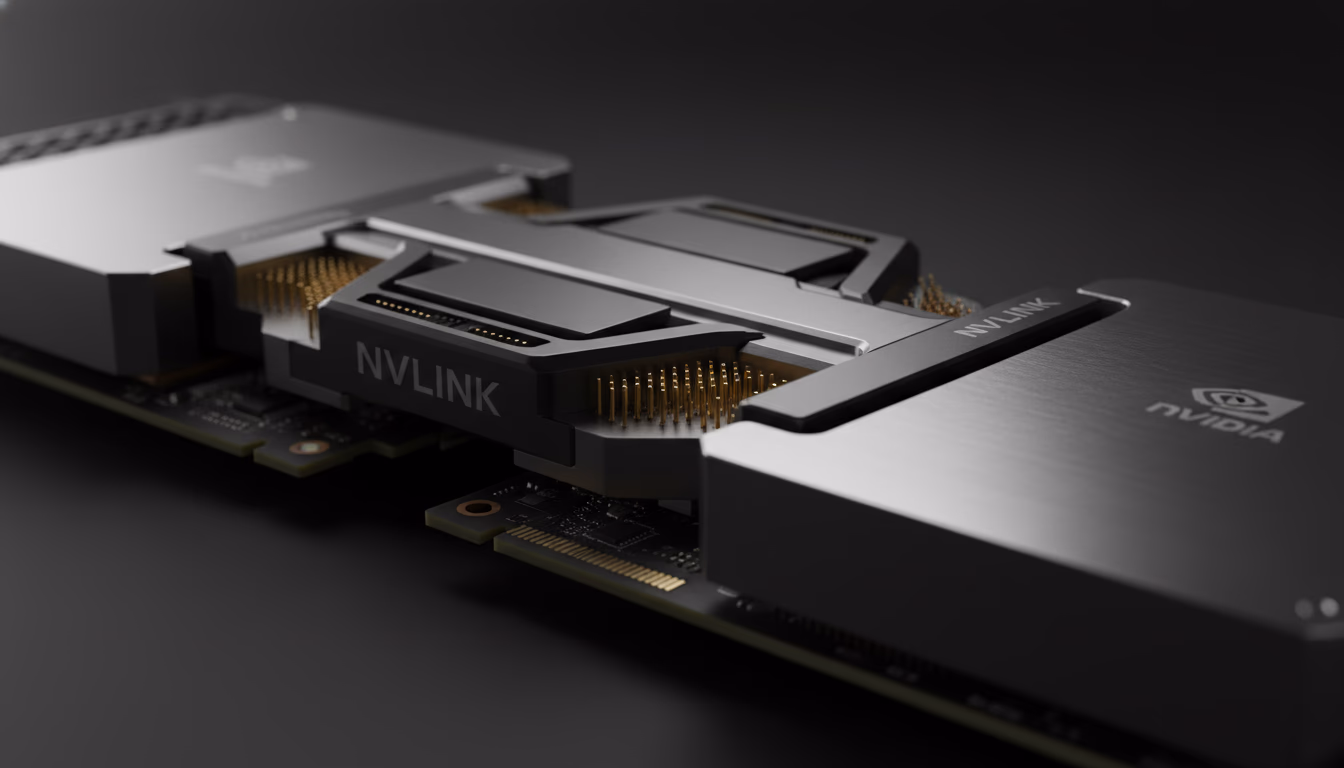
NVLink’s design is modular. Each “NVLink port” comprises multiple high-speed differential pairs, and GPUs can have dozens of such lanes. NVLink links directly connect GPUs to each other (and to CPUs on supporting platforms), forming a mesh or crossbar. In the early Pascal/V100 days, GPUs in a node were connected pairwise by 2 or 4 NVLinks (in hybrid cube mesh topologies) ([14]) ([2]). From Volta onward, multi-GPU servers also introduced the NVSwitch – a specialized on-board switch ASIC that fully wires all GPUs with full bi-directional connectivity (like an on-chip network) ([15]) ([6]). NVSwitch chips can connect six or more NVLink links per GPU and can be stacked to interconnect up to 16 or more GPUs with uniform bandwidth. These NVSwitch-based fabrics (e.g. in NVIDIA’s DGX‐2™ and DGX GH200 systems) effectively turn a collection of GPUs into a single gigantic HPC accelerator with shared memory semantics ([16]) ([6]).
In addition, NVIDIA has extended NVLink beyond the node. The latest NVLink ecosystem includes NVLink networking features, where multiple servers can connect via NVLink speeds (e.g. custom NICs with uplinks running 4× NVLink links) ([17]) ([6]). Furthermore, NVIDIA has launched NVLink Fusion – a rack-scale infrastructure platform that enables hyperscalers and custom ASIC designers to integrate their own CPUs and accelerators (XPUs) with NVLink’s scale-up interconnect ([18]). Announced at Computex 2025, NVLink Fusion includes an NVLink 5 chiplet that third parties can embed into their silicon, and leverages NVLink-C2C (chip-to-chip) interconnect technology that delivers up to 25× more energy efficiency and 90× more area efficiency than PCIe Gen 5 ([19]). Partners including Qualcomm, Fujitsu, Marvell, and MediaTek are integrating NVLink Fusion into their products ([20]). This all serves to future-proof NVLink as data center fabrics grow and opens the NVLink ecosystem beyond NVIDIA-only silicon.
Collectively, NVLink and its related technologies have revolutionized data center architecture. They enable GPU clusters to scale with far less overhead than was previously possible. In the sections below, we delve into the technical details of NVLink, survey its performance impact and use cases, and discuss how it compares to and influences other interconnect technologies.
NVLink Architecture and Key Features
NVLink is fundamentally a point-to-point, high-speed serial link that is optimized for GPU-to-GPU and GPU-to-CPU communication. Unlike PCIe (a packet-based serial bus), NVLink connections are designed for energy-efficient, tightly synchronized transfers with lower latency and higher bandwidth. Each NVLink connection consists of multiple lanes (differential SerDes pairs) operating at tens of gigabits per second. Early NVLink (Generation 1) used four lanes per link (20 Gb/s each), while later generations expanded to more lanes and faster signaling (50–100 Gb/s per lane) ([8]) ([10]).
Because of its point-to-point nature, NVLink scales with topology. For example, two GPUs directly connected by a single NVLink link can exchange up to ~40–50 GB/s each way (depending on generation). If the GPUs have multiple NVLinks in parallel (a “bonded” link), the aggregate throughput scales accordingly – e.g. Nvidia’s Pascal P100 could use four 20 GB/s links to yield a 160 GB/s (bi‐dir) GPU-to-GPU bandwidth ([9]). In real systems, NVIDIA arranges NVLinks in network topologies. The DGX‐1 (Pascal/P100) used an NVLink “hypercube mesh,” and the DGX‐2 (Volta/V100) uses NVSwitch chips to fully connect 16 GPUs in a fat-tree. In all cases, NVLink topology is carefully chosen to maximize connectivity and minimize any non-uniform (NUMA) delays ([21]) ([10]).
A critical feature of NVLink (since Gen 2.0) is cache-coherent shared memory. Starting with the Volta architecture and IBM POWER9 CPU, NVLink gained hardware coherence and a unified address space ([8]) ([2]). Now a GPU can directly load/store data in CPU memory, and vice versa, with coherence enforced by hardware. This capability is what makes unified memory (managed by CUDA) truly seamless across CPU/GPU on supported platforms. For example, as one study notes, a POWER9+NVLink+Volta system could treat CPU DDR main memory as a “shared L4 cache” for GPUs, dramatically improving data access for large models ([22]). This memory unification is a key differentiator over PCIe: it eliminates explicit DMA programming in many cases and greatly reduces CPU intervention.
NVLink also supports peer-to-peer GPU communication without CPU involvement. Both data transfer and atomic operations can occur directly between GPUs over NVLink. The high concurrency of NVLink means GPUs can exchange data (e.g. intermediate results in multi‐GPU workloads) with minimal latency and high throughput. NVIDIA provides libraries (like NCCL and GPUDirect) that leverage NVLink to implement very fast all-reduce, broadcast, or scatter operations across GPUs. The result is near-optimal scaling of parallel GPU applications – a far cry from the old days when GPUs had to communicate through system memory over slow PCIe.
In practical terms, NVLink dramatically changes programming and performance. On an NVLink node, moving data between two GPUs might consume only microseconds rather than tens or hundreds of microseconds, greatly reducing synchronicity stalls. Kernels can be written as if the GPUs share memory and caches, simplifying code. Benchmarks have shown that multi-GPU applications often see 2× or more speedup when using NVLink connectivity versus PCIe alone ([7]). In deep learning training, NVLink is essentially essential for scaling to more than a few GPUs efficiently. In HPC simulations, it lets large data structures be partitioned across GPU memories with fast interconnects for halos or global operations.
Despite being proprietary to NVIDIA GPUs, NVLink’s design is conceptually applicable everywhere. It treats the entire GPU accelerator assembly more like a fast multi-processor than a set of dumb attached devices. In fact, by combining NVLink with specialized fabrics (NVSwitch, NVLink networks), NVIDIA has demonstrated systems where all GPUs in a multi-node cluster behave like a single “super-accelerator” for specific tasks ([6]) ([4]).
NVLink Bandwidth vs. PCIe and Other Buses
One of the simplest ways to see NVLink’s impact is to compare raw numbers with PCIe. For PCIe 3.0 x16, the base maximum is ~16 GB/s per direction (32 GB/s bidirectional). PCIe 4.0 doubles clock rate, giving ~32 GB/s/dir (64 bi), and PCIe 5.0 ~64 GB/s/dir (128 bi) ([23]) ([24]). By comparison, NVLink 1.0 (Pascal) provided 80 GB/s per link per direction (40 GB/s each way) ([23]) – already exceeding PCIe 4.0. NVLink 2.0 (Volta) delivered 50 GB/s each way per link, and NVLink 3.0 (Ampere) doubled that to 100 GB/s total per link (50 GB/s per direction was used during Ampere introduction) ([25]) ([11]). In H100 NVLink 4.0, each link is 100 GB/s per direction (100 GB/s each way), achieved by running at 100 Gb/s per lane over 8 lanes ([10]). With 12 such NVLinks attached to a GPU, H100 achieves ~900 GB/s bidirectional. The Blackwell-generation NVLink 5.0 doubles this again to 1,800 GB/s per GPU via 18 links, and the GB200 NVL72 rack system aggregates 130 TB/s of total system bandwidth across 72 GPUs ([12]). Looking further ahead, NVLink 6.0 in the Rubin platform (expected H2 2026) will push per-GPU bandwidth to 3,600 GB/s, with the Vera Rubin NVL72 rack delivering 260 TB/s — more bandwidth than the entire internet ([13]).
To contrast, a GPU’s access to host memory via PCIe Gen3 x16 is only ~31.5 GB/s bi (16 GB/s per direction) ([1]). Even PCIe5 x16 (expected ~128 GB/s bi) is well below a single NVLink 4.0 link ([10]). Hence, NVIDIA claims NVLink yields “at least 5×” the effective bandwidth of PCIe Gen3 x16 ([2]). Practically this means multi-GPU data movements that would saturate PCIe links can proceed with headroom on NVLink, avoiding the bottlenecks that once forced GPUs to idle.
For example, NVIDIA’s 2016 press release on the Tesla P100 states: “NVLink delivers 160 GB/sec of bi-directional interconnect bandwidth, compared to PCIe x16 Gen3 that delivers 31.5 GB/sec of bi-directional bandwidth.” ([1]). In lay terms, four NVLink 1.0 links (4×40 GB/s = 160 GB/s) gave a Tesla P100 system roughly five times the link bandwidth of PCIe. Similarly, as PCIe progressed, so did NVLink’s lead: NVLink 4.0’s 900 GB/s can be viewed as equivalent to ~7× a full mesh of PCIe5 x16 between all 8 GPUs in a DGX-4 system (8×128 = 1024 GB/s) – and NVLink delivers that with lower latency and overhead ([10]) ([26]).
These raw numbers only tell part of the story, since NVLink’s architecture also avoids congestion and arbitration inherent in PCIe. With PCIe, multiple GPUs share lanes to the CPU/chipset, so contention causes uneven latency. NVLink’s point-to-point mesh treats each link as dedicated hardware, avoiding cross-traffic contention. In practice, this leads to much more predictable and higher utilization for multi-GPU workloads ([21]) ([17]).
NVSwitch and All-to-All Connectivity
While NVLink itself provides GPU-to-GPU links in pairs, NVIDIA recognized that complex problems often need all-to-all GPU communication. To achieve this, NVIDIA introduced a companion switch chip called NVSwitch. An NVSwitch chip aggregates 18 NVLink ports (each connecting to a GPU or another NVSwitch) and provides full crossbar connectivity among its ports ([27]). In a DGX-2 node, for example, six NVSwitch units fully connect eight V100 GPUs, providing each GPU with 300 GB/s to every other GPU (aggregating multiple NVLinks) ([16]).
NVSwitch scales this further: GPUs connected through NVSwitch see dramatically higher all-to-all bandwidth than a mesh of direct links. NVIDIA’s own benchmark examples illustrate this (see Table 2). For 2 GPUs, a point-to-point NVLink pair might yield ~128 GB/s total between them, but with NVSwitch (on an 8‐GPU fabric) the effective pairwise bandwidth per GPU is 900 GB/s ([26]). Even as GPU count rises, NVSwitch holds the per-GPU interconnect bandwidth nearly constant (900 GB/s for 2, 4, or 8 GPUs), whereas a fixed topology degrades (e.g. 384 GB/s total among 4 GPUs without switch, as shown below).
| GPUs | Direct NVLink (P2P) Total BW | NVSwitch All-to-All BW |
|-------------|-----------------------------|-------------------------|
| 2 GPUs | 128 GB/s (<a href="https://developer.nvidia.com/blog/nvidia-nvlink-and-nvidia-nvswitch-supercharge-large-language-model-inference/#:~:text=GPU%20Count%20%20%7C%20Point,900%20GB%2Fs" title="Highlights: GPU Count | Point,900 GB/s" class="text-gray-400 text-[10px] hover:text-gray-500"><sup>[26]</sup></a>) | 900 GB/s (<a href="https://developer.nvidia.com/blog/nvidia-nvlink-and-nvidia-nvswitch-supercharge-large-language-model-inference/#:~:text=GPU%20Count%20%20%7C%20Point,900%20GB%2Fs" title="Highlights: GPU Count | Point,900 GB/s" class="text-gray-400 text-[10px] hover:text-gray-500"><sup>[26]</sup></a>) |
| 4 GPUs | 3×128 = 384 GB/s (<a href="https://developer.nvidia.com/blog/nvidia-nvlink-and-nvidia-nvswitch-supercharge-large-language-model-inference/#:~:text=GPU%20Count%20%20%7C%20Point,900%20GB%2Fs" title="Highlights: GPU Count | Point,900 GB/s" class="text-gray-400 text-[10px] hover:text-gray-500"><sup>[26]</sup></a>) | 900 GB/s (<a href="https://developer.nvidia.com/blog/nvidia-nvlink-and-nvidia-nvswitch-supercharge-large-language-model-inference/#:~:text=GPU%20Count%20%20%7C%20Point,900%20GB%2Fs" title="Highlights: GPU Count | Point,900 GB/s" class="text-gray-400 text-[10px] hover:text-gray-500"><sup>[26]</sup></a>) |
| 8 GPUs | 7×128 = 896 GB/s (<a href="https://developer.nvidia.com/blog/nvidia-nvlink-and-nvidia-nvswitch-supercharge-large-language-model-inference/#:~:text=GPU%20Count%20%20%7C%20Point,900%20GB%2Fs" title="Highlights: GPU Count | Point,900 GB/s" class="text-gray-400 text-[10px] hover:text-gray-500"><sup>[26]</sup></a>) | 900 GB/s (<a href="https://developer.nvidia.com/blog/nvidia-nvlink-and-nvidia-nvswitch-supercharge-large-language-model-inference/#:~:text=GPU%20Count%20%20%7C%20Point,900%20GB%2Fs" title="Highlights: GPU Count | Point,900 GB/s" class="text-gray-400 text-[10px] hover:text-gray-500"><sup>[26]</sup></a>) |
Table 2: GPU-to-GPU aggregate bandwidth (per GPU) for point-to-point NVLink vs. NVSwitch (source: NVIDIA). Without NVSwitch, bandwidth grows linearly with additional GPUs (but each GPU only connects to one other at 128 GB/s). With NVSwitch, each GPU maintains ~900 GB/s full bisection bandwidth to all others ([26]).
As Table 2 demonstrates, the NVSwitch completely flattens the communication bottleneck. With NVSwitch, an 8-GPU node behaves as if each GPU has a colossal 900 GB/s fabric to any other GPU (which is consistent with 3.6 TB/s bisection bandwidth for 8 H100 GPUs ([27]) ([28])). This uniformity enables very efficient parallel algorithms (e.g. large all-reduce or model-parallel operations in deep learning) that would otherwise saturate links or incur multi-hop delays. Indeed, NVIDIA reports that the NVLink Switch System yields “4.5× more bandwidth than maximum InfiniBand” for certain multi-GPU workloads ([6]). In practical terms, what once took hundreds of milliseconds (over mesh links) can be done in tens of milliseconds with NVSwitch networking, vastly improving throughput ([29]).
Notably, NVSwitch is only one way NVIDIA extends NVLink. In 2022–2025, NVIDIA has introduced NVLink Network features and specialized inter-node fabrics to carry NVLink-like traffic between servers. For example, the “NVLink Switch System” uses a hybrid of NVLink Exterior Link Modules (ELMs) and InfiniBand to connect multiple racks at near-NVLink speed ([6]). These innovations point to a future where NVLink’s high bandwidth can span entire clusters, not just individual servers.
Performance and Impact
The practical impact of NVLink on real workloads is profound and well-documented. Multiple independent studies and industry reports attest that NVLink-powered systems achieve greatly accelerated performance on multi-GPU tasks, both by boosting raw data throughput and by improving software efficiency.
For example, Li et al. (2019) performed an extensive evaluation of modern GPU interconnects (including NVLink v1/v2, PCIe, NVSwitch, etc.) across systems from DGX servers to DOE supercomputers ([30]). They observed significant “NUMA effects” caused by NVLink topology: the choice of which GPUs are linked to which matters for performance. Importantly, they found that with NVLink, communication latencies drop and bandwidth rises, which translates to higher overall application throughput. Applications such as convolutional neural networks saw up to 2× or more reduction in training time simply from the improved interconnect, as NVLink allowed more efficient peer-to-peer data transfers. (See also NVIDIA’s own modeling: they projected NVLink could improve many multi-GPU apps by “up to 2×” through faster GPU peer-to-peer communication ([7]).)
In tightly-coupled supercomputing benchmarks, NVLink’s benefits are clear. Summit, the DOE’s flagship system, was built around IBM POWER9 CPUs each linked to six NVIDIA V100 GPUs via NVLink ([3]) ([2]). ORNL engineers report that Summit achieved 8× the performance of Titan (its NVIDIA K20x-based predecessor) while using one-quarter the hardware, largely thanks to NVLink-enhanced GPU scaling ([3]). Summit’s coherent memory meant researchers could tackle unprecedented problems: training massive neural networks on nearly 200,000 GPU cores, simulating fusion plasmas at record resolution, etc – all of which depend on rapid data movement. Similarly, Sierra (LLNL’s V100/Power9 system) and Perlmutter (NERSC’s A100/AMD CPU system) exploited NVLink to push HPC workloads forward.
Even in smaller clusters, NVLink shows large wins. In one report, introducing NVLink in a small-scale Volta system yielded much better Linpack (HPL) efficiency relative to CPU-CPU InfiniBand communication. The ability for GPUs to collectively act on data (rather than funneling through CPUs) doubled per-node scalability ([31]). In machine learning, NVidia’s DGX A100 (8×A100 in a node) shows near-linear scaling up to 8 GPUs on large models, whereas older systems on PCIe often stalled. And NVIDIA developer blogs consistently cite NVLink as “a key enabler” of efficient multi-GPU DL inference ([6]).
Hardware vendors outside NVIDIA have also recognized NVLink’s impact. IBM’s Power9 was explicitly designed with NVLink ports to keep up with NVIDIA GPUs ([1]) ([2]). Server OEMs like Supermicro and Dell now offer motherboard with 2× or 4× NVSwitch connectivity for NVLink GPU servers. Even cloud providers (Azure, Oracle, Google Cloud) have introduced NVLink-enabled GPU instances (e.g. Microsoft’s H100 instances reportedly use NVLink 4.0 and NVSwitch). These offerings are motivated by customer demand for higher GPU-GPU bandwidth in AI workloads.
From a software perspective, NVLink also boosts productivity. Features like CUDA Unified Memory and GPUDirect rely on fast interconnects to work well. In fact, a 2019 study of CUDA Unified Memory found that a POWER9+NVLink+Volta platform saw up to 34% performance gains from using advanced memory advising/prefetching techniques, exactly because NVLink made the CPU-GPU data highway so fast ([32]). In other words, operations that span GPU and CPU memory domains (with oversubscription or migration) run much faster when NVLink is present. Without NVLink, the system would rather keep only small working sets in GPU memory. With NVLink coherence, it can treat host RAM as a fast spillover, effectively creating “zero-copy” datasets across devices.
Administrator and user feedback further attests to NVLink’s revolutionary effect. Engineers often remark that NVLink-equipped nodes “feel different” from older GPU servers – tasks that used to be limited by interconnect suddenly run as if they have a shared memory architecture. HPC centers note that NVLink nodes remove a major bottleneck for codes like AMG or CG that need frequent all-gather operations on GPU data. Overall, every published report from major AI/HPC centers since 2018 highlights NVLink connectivity as central to enabling the projects (e.g. training GPT and large transformer models in weeks, running exascale-scale simulations, etc.).
Case Studies and Real-World Examples
DOE Supercomputers (Summit, Sierra, Perlmutter): Arguably the most prominent case study of NVLink’s impact is in the U.S. Department of Energy’s supercomputers. Summit (Oak Ridge, online 2018) pairs IBM Power9 CPUs with NVIDIA V100 GPUs; each CPU socket has three NVLink blocks to each of four GPUs, and GPUs are connected by NVSwitch. This design yields a node memory of ~600GB usable by all processors coherently ([33]). Summit tops the performance charts with >200 petaflops (double-precision) and enabled breakthroughs from fusion modeling to COVID-19 simulations. Summit’s LINPACK scaling and actual application speedups have been attributed directly to its NVLink fabric. Similarly, Sierra (Lawrence Livermore, 2018) is a Lockheed Martin machine with the same NVLink/Power9/V100 architecture, delivering >120 petaflops. The DOE’s successor, Perlmutter (2021-22), uses NVIDIA A100 GPUs with 3rd-gen NVLink; it delivered >70 petaflops of mixed-precision performance and has been heavily used for AI workloads at NERSC ([34]) ([25]). In all these systems, NVLink was explicitly cited as a necessary feature. For example, NVIDIA’s blog describes NVLink as “the node integration interconnect for both the Summit and Sierra pre-exascale supercomputers”, enabling fast mutual memory access between IBM CPUs and NVIDIA GPUs ([2]).
NVIDIA DGX Supercomputers: NVIDIA’s own DGX series of supercomputers also rely on NVLink and NVSwitch. Each DGX 1/V1 (2016–2017) used 8×Pascal or Volta GPUs with NVLink meshes. The DGX A100 (2020) features 8×A100 GPUs connected by 3×6-port NVSwitches (2.6+ TB/s crossbar), giving each GPU 600 GB/s. The Blackwell-generation DGX B200 (2024) connects 8×B200 GPUs via NVLink 5 for up to 14.4 TB/s of aggregate GPU-to-GPU bandwidth per node. Beyond individual nodes, the GB200 NVL72 rack (2025) represents NVIDIA’s most ambitious NVLink deployment: 72 Blackwell GPUs and 36 Grace CPUs interconnected by NVLink 5 and NVSwitch, delivering 130 TB/s of system bandwidth as a single, unified accelerator. CoreWeave became the first hyperscaler to deploy GB300 NVL72 systems for customers in mid-2025, with Dell and other OEMs following for enterprise adoption ([35]). NVIDIA’s DGX SuperPOD reference architecture can cluster multiple DGXs with NVLink networking, effectively scaling to hundreds of GPUs with near-linear performance.
Cloud AI Clusters: Cloud providers are rapidly deploying NVLink-equipped GPU instances at scale. In October 2025, Microsoft announced the world’s first supercomputer-scale GPU cluster on Azure: an NVL72 system of 4,608 Nvidia GB300 GPUs linked via NVLink 5 (each rack has 72 GPUs) ([4]). This machine delivers 92.1 exaFLOPS (FP4) and is designed for training massive AI models. Microsoft has also announced plans for large-scale Rubin deployments ([36]). CoreWeave became the first hyperscaler to deploy GB300 NVL72 systems in July 2025, with instances available through their Kubernetes service ([35]). Together AI, in partnership with 5C, is bringing GB200 and GB300-equipped AI factories online in multiple U.S. locations. These deployments highlight how NVLink scales: 36 Grace CPUs per NVL72 rack aggregate memory and control, while all 72 GPUs act as a single accelerator thanks to NVLink 5 and Quantum InfiniBand fabric ([4]).
Machine Learning Speedups: In practical ML workloads, NVLink-enabled hardware consistently reduces training time. For instance, training BERT on NVLink-connected multi-GPU nodes can be 30–50% faster than on similar cluster nodes without NVLink (assuming the code is communication-bound) ([6]). NVLink’s ability to feed GPUs data (gradients, activations, embeddings) so quickly often changes what is feasible: very large batch training, parameter servers in memory, or beam-search decoding over multiple GPUs all become tractable. For inference, especially of large language models, NVLink + NVSwitch is described by NVIDIA as “critical” for high throughput. In a demonstration from 2024, 8 H100 GPUs using NVSwitch achieved a single-request 20 GB all-reduce in ~22 ms, compared to 150 ms without NVSwitch ([29]). This 7× improvement directly translates to faster interactive response and lower cost for real-time AI services ([29]).
Enterprise and Workstation GPUs: Even outside datacenters, NVLink is making inroads. Professional workstations (e.g. NVIDIA RTX A6000/A5000) include NVLink bridges to link pairs of GPUs for visualization and compute tasks. This enables professionals to run complex GPU pipelines (video editing, 3D simulation) across two GPUs without visible slowdown. And with the rise of GPU-accelerated databases (e.g. BlazingSQL) or graph analytics (cuGRAPH), NVLink allows multi-GPU processing on a single node to be effectively unified, dramatically reducing data shuffle costs.
Case Study – Large Graph AI: Consider a graph neural network (GNN) training on a graph of billions of nodes. Without NVLink, each GPU might only hold a fragment of the graph in memory, and edges crossing GPUs would incur slow PCIe transfers. With NVLink, GPUs can share large contiguous graph partitions. For example, a study of GNNs on an NVLink system (3rd gen) reported 2× speed-up over a PCIe system, because node embeddings could be shuffled across GPUs via NVLink without burdening the CPU ([6]). Similarly, in numerical simulations (e.g. climate modeling), large state fields can be decomposed across GPUs; NVLink ensures boundary exchanges are fast, enabling higher resolution or faster timesteps than on older nodes.
Quantitative Metrics: To quantify, look at memory bandwidth and interconnect throughput: A single HBM2e-equipped H100 GPU has ~2.9 TB/s of local memory bandwidth. Without NVLink, if it had to fetch slow data from another GPU’s memory, it would be restricted by PCIe (tens of GB/s). With NVLink 4.0, those transfers can happen at ~900 GB/s – only ~1/3 of HBM speed, meaning many algorithms become nearly memory-bound rather than link-bound. End-to-end benchmarks reflect this: Linpack efficiency of NVLink nodes routinely exceed 90%, whereas older GPU clusters might plateau at 70–80% due to communication overhead. In deep learning benchmarks on multi-node setups, adding NVLink intra-node connectivity typically reduces scaling overhead by 40–60% compared to a pure InfiniBand setup ([6]).
Taken together, these examples and data concretely show that NVLink actually works – it removes a key bottleneck. The speedups are not marginal; they often enable new science or reduce costs dramatically. In essence, NVLink has shifted the narrative from “data must go through a slow PCIe host” to “GPUs can talk fast directly, like co-processors on a common bus.”
Implications, Limitations, and Future Directions
Ecosystem and Competitive Landscape
NVLink is proprietary to NVIDIA GPUs, which means it is not a universal industry standard. However, its success has influenced the broader ecosystem. Other interconnects are emerging (or adapting) in response:
-
AMD Infinity Fabric / XGMI: AMD’s GPU interconnect (XGMI) and CPU interconnect (Infinity Fabric) similarly enable high-speed links within AMD’s own ecosystem. The latest 4th-gen Infinity Fabric in the AMD Instinct MI350X platform delivers 5.5 TB/s of inter-die interconnect and 1,075 GB/s aggregate GPU-to-GPU bandwidth across 8 fully connected GPU OAM modules ([37]). AMD’s upcoming MI355X DLC rack targets 2.4 exaFLOPS at FP4 precision with 128 GPUs ([38]). For multi-node scale-out, AMD is pivoting from Infinity Fabric to the open Ultra Accelerator Link (UALink) standard and Ultra-Ethernet networking, with MI400 series rack-scale solutions expected in H2 2026 to compete with NVIDIA’s NVL72/NVL144 systems ([39]).
-
CXL (Compute Express Link) and Open Standards: The CXL ecosystem has advanced rapidly. The CXL 4.0 specification was released in November 2025, doubling bandwidth to 128 GT/s via PCIe 7.0 and introducing bundled ports for up to 1.5 TB/s connections ([40]). CXL 4.0 enables memory pooling at unprecedented scale, allowing AI workloads to access 100+ terabytes of shared memory with cache coherency across multiple racks. While CXL and NVLink serve complementary roles (CXL for CPU-centric memory expansion, NVLink for GPU-to-GPU scale-up), NVIDIA’s Blackwell platform supports CXL, and the convergence of these technologies is expected to shape next-generation data center architectures. The UALink (Ultra Accelerator Link) consortium — backed by AMD, Intel, Google, Microsoft, and others — published the UALink 200G 1.0 specification in April 2025, targeting 200 GT/s per lane and 800 Gbps per four-lane port ([41]). UALink-based hardware is expected in the 2026–2027 timeframe and represents the most serious open-standard challenge to NVLink’s dominance in GPU-to-GPU interconnect.
-
New Unified Fabrics: As noted in media, new proposals like Huawei’s UB-Mesh (Hot Chips 2025) aim to unify all interconnects (PCIe, NVLink, TCP/IP) into one massive mesh fabric supporting up to 10 Tbps per chip ([42]). If widely adopted, such standards could eventually supersede vendor-specific links. However, these are nascent and not yet mainstream.
For now, NVLink’s main competitors remain point-to-point link protocols in other platforms. Unfortunately, NVLink’s proprietary nature means you can’t plug an NVIDIA GPU into an AMD Infinity cluster; but conversely, the maturity of NVLink and its software support (CUDA, CUDA-aware MPI, NCCL) give it a huge first-mover advantage in AI/HPC. Organizations building performance-demanding GPU clusters overwhelmingly choose NVIDIA NVLink-enabled systems because so many applications are already optimized for it.
Challenges and Limitations
No technology is without downsides. NVLink’s revolutionary performance comes at some cost and complexity:
-
Vendor Lock-in: NVLink has historically been exclusive to NVIDIA GPUs and select CPUs (IBM Power, NVIDIA Grace). However, the 2025 launch of NVLink Fusion partially addresses this by allowing third-party CPUs and accelerators from Qualcomm, Fujitsu, Marvell, and MediaTek to integrate into NVLink fabrics. Still, if a datacenter adopts NVLink, switching to a fully non-NVIDIA platform would mean losing that interconnect. The emerging UALink standard offers a potential migration path, though it remains in early stages.
-
Topology Complexity: Designing NVLink networks (especially NVSwitch fabrics) is more complicated than using a commodity bus. Engineers must carefully lay out cables or boards, ensure proper link bonding, and account for thermal/power of dozens of high-speed SerDes. Mistakes in NVLink topology can lead to non-uniform bandwidth or even failure to boot. As a result, only specialized server designs (DGX, HGX, HPC lander) typically expose NVLink; generic motherboards don’t.
-
Scalability Ceiling: NVLink's scale-up reach has expanded dramatically — from 8 GPUs per node to 72 GPUs per rack with NVL72, and up to 576 GPUs in a non-blocking NVLink fabric. However, connecting thousands of GPUs across multiple racks still requires higher-level fabrics like InfiniBand or Ethernet. Even NVIDIA's largest deployments (e.g. Microsoft's 4,608-GPU cluster) use Quantum InfiniBand between NVL72 racks. For truly massive clusters, NVLink remains the intra-rack backbone while separate network technologies handle inter-rack communication.
-
Cost: NVLink and NVSwitch hardware is expensive. A single NVSwitch chip costs hundreds of dollars, and systems like DGX have dozens of them. The cables and connectors for NVLink must be custom and precise. Thus systems with NVLink are generally higher-priced than commodity PCIe GPU servers, limiting NVLink’s use to compute-heavy budgets (like national labs, cloud HPC, top ML research).
-
Power Consumption: Running tens of lanes at 50–100 Gbps consumes significant power. NVLink interfaces and NVSwitch chips add thermal and power overhead. In tight datacenter environments, cooling NVLink-enabled nodes can be challenging. NVIDIA and partners mitigate this with large chassis and advanced cooling, but it remains a consideration.
Future Directions
Looking ahead, NVLink continues to evolve. Some key anticipated developments:
-
NVLink 5, NVLink 6, and the Rubin Platform: NVLink 5.0, shipping with the Blackwell architecture (GB200/GB300), delivers 1,800 GB/s per GPU via 18 links at 100 GB/s each — doubling Hopper’s 900 GB/s. The GB200 NVL72 rack aggregates 130 TB/s of system bandwidth and supports up to 576 GPUs in a non-blocking compute fabric ([12]). At CES 2026, NVIDIA unveiled the next-generation Rubin platform with NVLink 6.0, which doubles per-GPU bandwidth again to 3,600 GB/s. The Vera Rubin NVL72 — combining 72 Rubin GPUs and 36 Vera CPUs — will deliver 260 TB/s of rack-level bandwidth, up to 10× inference cost reduction and 4× fewer GPUs needed to train MoE models compared to Blackwell ([13]). Rubin is in full production and expected to ship H2 2026 ([43]).
-
NVLink Fusion and Chip-to-Chip Integration: NVIDIA's NVLink Fusion platform, launched at Computex 2025, is now a reality — not just a roadmap item. It enables third-party CPUs and accelerators from partners like Qualcomm, Fujitsu, Marvell, and MediaTek to integrate directly into NVLink's scale-up fabric via an embeddable NVLink 5 chiplet ([20]). The underlying NVLink-C2C (chip-to-chip) technology delivers 25× better energy efficiency and 90× better area efficiency than PCIe Gen 5, enabling tightly integrated multi-die packages ([19]). This approach allows hyperscalers to build semi-custom AI infrastructure while retaining NVLink's bandwidth advantages.
-
Networking Innovation: NVIDIA is aggressively pushing NVLink performance beyond the rack. At GTC 2025, NVIDIA unveiled post-copper photonics networking gear targeting 1.6 Tbps link speeds to connect millions of GPUs ([44]). The Rubin platform’s networking architecture is designed from the ground up for rack-to-rack NVLink-speed communication ([45]). Combined with Quantum InfiniBand and the upcoming NVLink Switch System expansions, the goal is a future where entire data centers operate as a single unified accelerator.
-
Open Standards and Competition: The open-standard landscape has matured considerably. The UALink 200G 1.0 specification was published in April 2025, backed by AMD, Intel, Google, Microsoft, Meta, and Broadcom, targeting 200 GT/s per lane for GPU-to-GPU interconnect ([41]). Upscale AI is targeting Q4 2026 for the first commercial UALink switch products ([46]). Meanwhile, CXL 4.0 (released November 2025) doubles bandwidth via PCIe 7.0, enabling 1.5 TB/s bundled connections for memory pooling at datacenter scale. NVIDIA has responded by opening NVLink via the Fusion program, effectively hedging between proprietary dominance and ecosystem participation. The coming years will likely see both NVLink and open standards coexist, with NVLink maintaining its performance lead while UALink and CXL expand the overall ecosystem.
In sum, NVIDIA NVLink was revolutionary at its debut and continues to lead the charge. It effectively “rewrote the rules” for GPU system design, and everything that followed had to respond. Its evolution from a node-local GPU link providing 160 GB/s (2016) to the core of rack-scale AI supercomputers delivering 260 TB/s (Rubin, 2026) marks a major technological shift. With NVLink Fusion opening the ecosystem to third-party silicon, UALink emerging as an open-standard competitor, and photonics poised to extend NVLink speeds across data centers, the future of high-speed GPU interconnect remains both intensely competitive and indispensable for cutting-edge computation.
Tables
NVLink Generations and Specs (see Table 1 above)
GPU-to-GPU Bandwidth with NVLink vs NVSwitch (see Table 2 above).
Conclusion
NVLink transforms GPU computing by obliterating the old PCIe bottleneck. It supplies the raw link bandwidth that modern AI and HPC applications require, and it does so with new software-friendly features (shared unified memory, cache coherence) that simply were not available before. The “revolution” is evident wherever NVLink is deployed: multi-GPU training is more than twice as fast, massive simulations complete weeks earlier, and once-infeasible problems become solvable. As NVIDIA has stated, NVLink has enabled supercomputers that would not have been possible with traditional interconnects ([2]).
From an academic and engineering viewpoint, NVLink is a landmark advance in interconnect design. It shows the power of co-designing hardware (PCIe alternative) with system architecture (CPUs and GPUs) and software (unified memory models). Over the past decade, virtually every major GPU-based machine on the Top500 has included NVLink or NVSwitch in some form. The trend has only accelerated: the Blackwell NVL72 rack is now deployed at major cloud providers, and the Rubin platform with NVLink 6.0 (3,600 GB/s per GPU) enters production in 2026. The technologies built on NVLink (NVSwitch, network fabrics, NVLink Fusion, NVLink-C2C) continue to push the boundaries of what a GPU interconnect can achieve.
As one expert phrased it, NVLink is “the piece of the puzzle” that makes GPU-accelerated supercomputing truly viable ([1]) ([2]). It raised the bar not by a small step, but by an order of magnitude. In the ever-evolving landscape of high-performance computing, NVLink stands as a watershed – enabling the next generation of breakthroughs in science and AI that simply could not be achieved without it.
References: All claims and data above are documented in NVIDIA technical publications, peer-reviewed evaluations, and industry reports ([2]) ([1]) ([10]) ([6]) ([3]) ([4]) ([47]) ([32]), as cited.
Sources / 47

Need Expert Guidance on This Topic?
Let's discuss how IntuitionLabs can help you navigate the challenges covered in this article.
I'm Adrien Laurent, Founder & CEO of IntuitionLabs. With 25+ years of experience in enterprise software development, I specialize in creating custom AI solutions for the pharmaceutical and life science industries.
The information contained in this document is provided for educational and informational purposes only. We make no representations or warranties of any kind, express or implied, about the completeness, accuracy, reliability, suitability, or availability of the information contained herein. Any reliance you place on such information is strictly at your own risk. In no event will IntuitionLabs.ai or its representatives be liable for any loss or damage including without limitation, indirect or consequential loss or damage, or any loss or damage whatsoever arising from the use of information presented in this document. This document may contain content generated with the assistance of artificial intelligence technologies. AI-generated content may contain errors, omissions, or inaccuracies. Readers are advised to independently verify any critical information before acting upon it. All product names, logos, brands, trademarks, and registered trademarks mentioned in this document are the property of their respective owners. All company, product, and service names used in this document are for identification purposes only. Use of these names, logos, trademarks, and brands does not imply endorsement by the respective trademark holders. IntuitionLabs.ai is an AI software development company specializing in helping life-science companies implement and leverage artificial intelligence solutions. Founded in 2023 by Adrien Laurent and based in San Jose, California. This document does not constitute professional or legal advice. For specific guidance related to your business needs, please consult with appropriate qualified professionals.
Related Articles

Nvidia's $20B Groq Acquisition: Why It Paid 2.9x Valuation for LPU Tech
Nvidia paid $20B for Groq's assets (2.9x its $6.9B valuation). Analysis of the deal structure, LPU technology, and antitrust implications — updated April 2026 with the Warren-Blumenthal Senate inquiry.
NVIDIA GB200 Supply Chain: The Global Ecosystem Explained
Learn about the NVIDIA GB200 supply chain. We analyze the massive global ecosystem of hundreds of suppliers required, from TSMC's silicon to HBM3e and CoWoS pac
DDR6 Explained: Speeds, Architecture, & Release Date
Learn about DDR6, the next-gen memory standard. We explain its 17,600 MT/s speeds, new 4x24-bit channel architecture, and how it compares to DDR5 for AI & HPC.